check near the DAC, re do some solder, and always the same thing
with nothing plugging 0V on A0 & A1, but if i plug a 0V CV signal in CVin1 A0 = 0.29V
if i have 0V on pin 10 of DAC, the problem is maybe near the opamp ?
I will return
check near the DAC, re do some solder, and always the same thing
with nothing plugging 0V on A0 & A1, but if i plug a 0V CV signal in CVin1 A0 = 0.29V
if i have 0V on pin 10 of DAC, the problem is maybe near the opamp ?
I will return
Sounds like (at least) two problems. Plugging in a 0 V CV should be exactly the same as not plugging in anything. Again, check that 0 V CV at points from the sequencer to the A0 pin to see where it becomes nonzero.
And if there is 0 V on DAC pin 10 and nonzero on the CV OUT, then there must be a separate problem in the output section:

If the jumper is in the 0–10V position (connecting J2 pins 1 and 2) then this is just a non inverting amplifier so 0 V at DAC_B should give 0 V at CV_OUT_B.
If 0 V at DAC pin 10, should be 0 V at TL072 pin 5, and at (either end of) R3, and (either end of) R9.
error pin 10 of DAC is for B not for A, i have not 0V on pin 14 so the problem go up to the arduino
new day new tests
i made all this test and the problem is really when I put a jack in the CVin (with or without cv), it is removing the connection to the GND of the jack which causes the arduino to send Voltage through the circuit
no jack = 0V
jack in = +? V (depending on the location measured) to the arduino:
cv out A / pin 3 opamp / pin 14 from the DAC / A0 on arduino
cv out B / pin 5 opamp / pin 10 from the DAC / A2 on arduino
as if the arduino had a continuous leak, but which goes to the GND through the jack, and when you cut the connection to the GND it appears
i’m lost
Thought you had nonzero output on both CVs? If you had 0 V on pin 10 and nonzero output for quantizer B then there’s an output stage problem.
On the input side, if you plug in a cable that is not connected to a CV source then you have a floating input and you can get unpredictable results. You can try adding a 100k pulldown resistor between each CV IN and ground. If I ever do a new version of dac/ino those will be there.
If you plug in a cable that is connected to a 0 V CV source, e.g. a sequencer (turned on and running with pots turned to 0), it should be the same as nothing plugged in. If not, measure voltage at:
Also the first four of these with the Arduino unplugged (if you socketed it).
yes, not zero on both
i don’t have zero in pin 10 (except if nothing is connected on CV1)
i will do this
it’s not the same at all
i mesured each time the seq cable CV (=0V) before pluging it for testing the Quantizer.
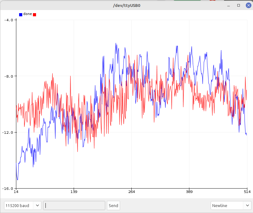
the problem is here, when i plug the jack, zero V become 1.98 …? on femal jack tip ( all the way opamp,dac, untill the arduino pin)
look good
A0 / A2 not good (not zero)
A1 / A3 seems good
here you suggest that i re do the mesure test with no arduino on socket and with power ?
thanks
Yes
What happens if you change the voltage coming out of the sequencer? What is it’s say 1 V (when not plugged into quantizer)?
it go between 0.89 (?) V to near 6/7 V
sorry i don’t understand what you mean
I re mesured without arduino
with a 0V CV signal (verified) in CVin1
for Quantizer 1
0.20V CVin1 femal jack Tip
0.20V CVinA on the board
0V pin 3 opamp
0V pin 14 DAC
0V CV out jack
for Quantizer 2
0.50V CVin1 femal jack Tip
0.50V CVinC on the board
0V pin 5 opamp
0V pin 10 DAC
0V CV out jack
the problem seems to come from the hardware between DAC and CVinput jack
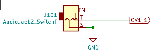
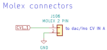
Here is everything from the CV1 IN jack of quantizer A to the A_IN line that connects to Arduino pin A0:
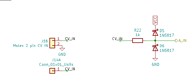
The only positive voltage source at all here is VCC at the cathode of D5, and of course that should not result in any voltage at A_IN. And besides, VCC comes from the +5 V pin on the Arduino (not an external regulator) so with the Arduino removed there should be no voltage there either. +12 V should connect to nothing but the voltage reference and the output op amp. Not to anything on the input side.
So it seems definite that positive voltage is somehow connected where it should not be somewhere in the components shown above. And if it were to the right of R22 it would appear at the Arduino regardless of whether the CV IN jack were connected to ground or not, so it would have to be to the left of R22, in the Molex connectors or the J14 header (which you probably don’t even have) or the jack itself.
Or, in spite of how it appears from everything you’ve done to check, the sequencer really isn’t putting out 0 V.
How about if you plug in a cable to CV1 IN and short the tip and sleeve together at the other end? Or if you plug in a cable and connect tip to sleeve with a 1k resistor? Or try other CV sources? And just to be sure, have you measured the CV1 IN voltage while connected to the sequencer with ±12 V power to the quantizer (but not the sequencer) turned off?
Just to verify your panel components: The CV1 IN jack should have connections:
Tip to 2 pin Molex connector (or solder direct to dac/ino board) (with other pin of Molex connected to ground)
Tip switch to ground
Sleeve to ground
No other connections
There should be continuity between ground on the dac/ino board and sleeve or tip switch.
yes all like that, and continuity test ok
i also try to change the jack, same thing
i don’t think that come from out of the quantizer, when i plug a jack with nothing at the other side (i know pulldown ![]() ) i have the same value in + (0.20V at A0, pin3 …), but i go test with another cv source
) i have the same value in + (0.20V at A0, pin3 …), but i go test with another cv source
a problem with my jacks wire somwhere ?
i put the resistors pulldown on CVs IN, after i tried with another CV source with the arduino on his socket and
ZERO VOLT !!!
i check and re check to be sure, and yes zero volt on the 2 CV output !! Half a victory
because i think that my seq have a problem
i tested with the seq and … … … ZERO VOLT on CVs output !!!
i not really understand, after hours, days of research and … i re check again and it seems to be OK, i hope that will be again the same thing tomorow when i put the power on (i’ma little affraid with that)
i don’t know if it’s the add of the resistors, put the power without the arduino, try with another cv … something mysterious
REALLY THANKS Rich to have pass all this time to help me 
PS : maybe here some magic pulldown resistors 
Some new test today and all works well now.
I’m not sure what are really solved the problem, but i’m very happy !!!
Hey, I was wondering if your quantizer needs any kind of calibration or if that is not needed because of the voltage reference? I was looking the somewhat simpler derivation of the HAWIGO quantizer, where it is stated:
The DAC has been replaced for a though hole MPC4821 DAC. Code for the Arduino has been adjusted to make it work with the new DAC. This PCB and Panel set is therefor for more advanced builders. The DAC has to be calibrated in code.
So, I was wondering if it would be easier for me to adjust the @analogoutput quantizer (I want less scales and less inputs and outputs, more like the hagiwo, but I don’t want to fiddle around with tables and a multimeter to “tune” the quantizer ![]() )
)
Not really sure what you (or Hagiwo) mean by calibration. Maybe just the output scale factor? To get 1 V/oct? The PCB has trimmers on the output stages to adjust the gain.
The REF02CP voltage reference has accuracy 1%, which isn’t good enough for V/oct. So an adjustment on the output gain (either via trimmer or software) is required. Substituting a REF02EN gets you 0.3%, which is likely good enough, though that’s an $11 part. I don’t know why the circuit I was cribbing from used the REF02 instead of an LM4040 which even in the AIZ version (0.1%) is only $3. With an LM4040AIZ and matched resistors in the output stage I’d guess calibration would not be an issue. (As for the MCP4821 it has an internal reference with 2% accuracy.)
Then there’s DAC nonlinearity, which is a whole other issue and is not very good in the MCP DACs — integral nonlinearity is 2 LSB typical and up to 12 LSB maximum with 12 bit resolution, so with a 5 V range it’s up to 5*12/4096*1200 = 17.5 cents error. I made no attempt to correct for that in the quantizer. There are much better 12 bit DACs on the market with max INL of 1 or 2 LSB, although they cost more, and good luck finding them with the current chip shortages.
Yes, that is what I meant! Maybe I asked this before, but if we use trimmers anyway, does the accuracy play a role at all?
Okai, and for the nonlinearity I could measure a dac and try to compensate, but it also works without? I think @tamasgal experimented with this as well, but I don’t know to which conclusion he came.
Yeah, the trimmers are there because the accuracy isn’t, just saying you could maybe simplify things with a more accurate reference. Though I kind of prefer having trimmers even if the design isn’t supposed to need them.
I’ve been experimenting a bit with software compensation for nonlinearity… In principle you can measure the output and then adjust the input to get the right output. Problems are (1) low resolution and nonlinearity in the ADC you measure the output with and (2) non invertability of the response function. There are techniques to work around the former and the latter can be handled so long as you don’t demand perfection. But on the whole I think it’d be a lot easier to just use a DAC that has the kind of specs the application calls for. And for some purposes and to some ears the MCP DACs’ specs are acceptable.
Okai, I understand, but I was wondering if I could get away with leaving out the reference source (just use the 5V from the arduino (or LM7805) and a trimmer, or will that get me into trouble? Maybe I need to breadboard this ![]()
I made a little table with different quantizers that came to mind, comparing what they did.
So far, I think I like the super sixteen way, because that takes care of non-linearity as well, I think, but it needs more of a user interface to be able to do it. I guess the simplest solution (for me) is the way of the Penrose (I really like its interface btw! But the switches are not cheap and also I would need to learn more music theory to be able to set scales ![]() )
)
| analogoutput | super sixteen (extralife) | Quinienl/Hagiwo | Kassutronics | Penrose (sonic potions) | |
|---|---|---|---|---|---|
| DAC | MCP4922 | MCP4822 | MCP4921 | arduino pwm | MCP4801 |
| voltage reference | REF02CP+ | none | none | LP2951N | none |
| calibration | output trimmer (output gain) needs to be adjusted for 1V/oct | calibrated by playing octaves, measuring with multimeter, and saving corrections for DAC in eprom | no calibration procedure described, but Quinienl wrote they had to adjust values in the code because they used a different DAC than Hagiwo | voltage reference needs to be trimmed to 5.34V first, then the output is checked with multimeter to read 0V and 5V and the trimmers for reference voltage and output offset(gain?) are set for best match. The manual claims you can get up to 2mV error (1mV is 1.2cents detuning, AS3340 usually has around 5mV tracking error) | output trimmer (output gain) needs to be adjusted for 1V/oct |
Depends on your goals. Since that 5 V is being used for power it’s more subject to fluctuations than a voltage reference would be. (For LM78L05 maximum load regulation is around half a percent.)
From what I’ve seen the nonlinearity of the 4922 isn’t a very smooth function of code number. The one I was looking at had multiple narrow peaks on one DAC and the other looked kind of like random noise, but reproducible and it also did have some wider peak and valley structure.
Calibration by octaves would take out some of the worst of that but would still leave worse nonlinearity than some other DACs. But again, that might be sufficiently good for your purposes.
I decided to go with the kassutronics PWM method for now, but I learned a lot about dacs over the last weeks xD
One more practical question: would you normal the inputs of the two channels together? If you normal the inputs, you could generate a second output at a fixed interval, like always having the the fifth at the second output (if you set the offset accordingly). Or if you normal the offset (second CV), you can offset/transpose both channels at the same time. I guess doing both at the same time does not make sense, right?
@lookmumnocomputer It’s been forever since I looked at that code so I dunno how much I can help… but I looked into it and at least in the version of the code I have, DACTOP apparently doesn’t do anything! It’s defined as 4095 as in the line you show, it’s mentioned in one comment, and it doesn’t occur anywhere else. So I’m baffled as to why changing it would have any effect.
On the PCB the CV outputs are configurable as 0 to 5 V, 0 to 10 V, or -5 to 5 V via jumpers. For the quantizer it should be configured as either 0 to 10 V or -5 to 5 V. I guess if you had it set up for 0 to 5 V it’d display the opposite problem from what you’re reporting so probably you have it set up right.
Have you verified the voltage on the VREF pins of the DAC (pins 11, 13) is +5 V?
hey cheers. yes i checked the dac, and came to the conclusion its all probably right as when off quantize mode it also mirrors the voltage coming out,
when checking on debug mode on the arduino i found the values going in only being half of the amount the scale table was saying.
so input value lets say is 410 an octave, (when it says an octave is 819).
i thought this was odd but looking at the tables of the scales and the notes, this matched the 410 instead of the 819, so as i said i just halved the DACTOP and that halved the note scale, so 410 was an octave instead of twice that. so 5 volts spans over half 2047 values and then 10 volts is 4095 values.
no idea, im not bothered as it all works for me now, what goes in matches what comes out, so the dac cant be running at twice the amount, so who knows
im just curious how i had a problem like this and no one else has. its very odd.
im just not gunna touch it now, and disrupt the quantizing gods haha ![]()