Yeah, I saw that mentioned on the MFOS site. And I know I’ll totally forget about it and confuse myself so considered adding a load resistor…but considering how infrequently I’d need it I still can’t be bothered to add LED’s and extra resistors.
Though…most of that was because I was out of space on my attempt to cram it into 35mm x 100mm. now that I’ve doubled that to 70mm x 100mm I should probably rethink leaving them off.
But at that point I’m more tempted to just run with your design
Though I see all your traces are on the front which isn’t great for home etching.
I’m curious how you did the 2mm traces though - I don’t see a net class setup for it. On mine I created a new net class with the wider traces and assigned it to the power nets. I do see an extra track width defined on yours…but I’m not sure how to use what when drawing a track without assigning it as a net class like I did.
(and searching online for kicad help so many things reference older versions it can be really confusing!)
I just click on the track width dropdown, select “Edit pre-defined sizes…”, create a new size (2 mm), and then select that with the width dropdown before drawing tracks.
… but in looking around I see that in Edit > Edit Track & Via Properties, in the rightmost dropdown under “Action” you can select “B.Cu” and click “OK” and it moves all the tracks to the back layer, which you might find useful.
Ha! I hadn’t even noticed the track width pulldown
Or the easy way to move tracks between layers. Nice!
Gotta love a piece of software that’s flexible enough to have multiple ways of doing things. I’m sure there’s a lot more I keep missing just because I’m already falling into habits of doing things the way I figured out the first time
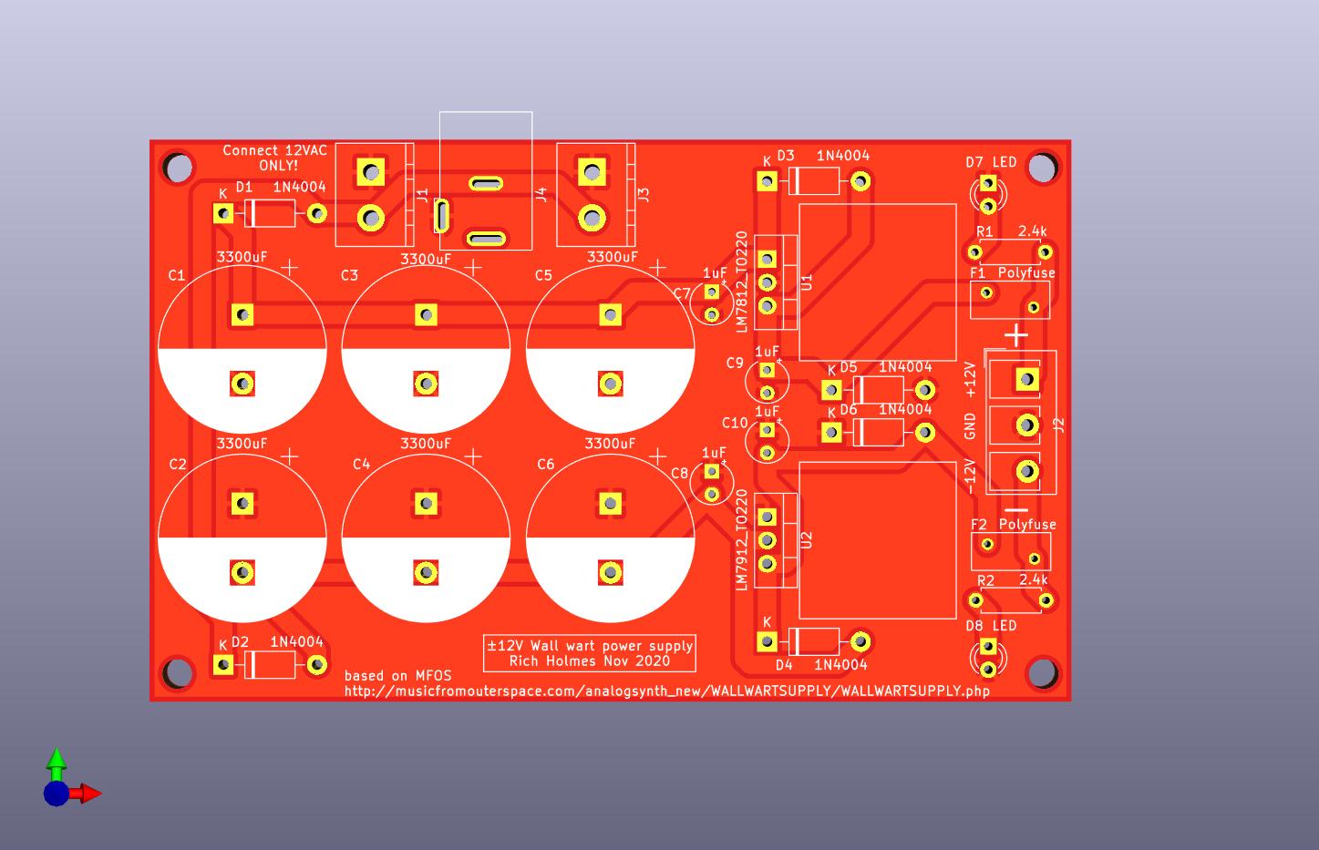
The tantalum caps became electrolytics, and there’s more differences. FC adds the LEDs and the 5V regulator. Big capacitors are different value, and capacitors after the regulators are much larger (100 µF instead of 1 µF). Of course the input and output connectors are different.
The main topology is basically the same, but there aren’t too many other options for it to be.
Yep, there’s nothing special about the PCB. A linear power regulator is one thing I’d expect to be better deadbugged than laid out on a board. It’s a simple circuit and as long as you place the heat sinks on the outside with decent air flow I don’t see where you could go wrong.
Hint: heat dissipation is how these circuits work. Just make sure the wasted heat has somewhere to go.
Yeah…there are only so many variations on a basic theme
The difference @analogoutput left off is MFOS has the regulators mounted to the board as a heatsink while the FC design uses separate heat sinks.
The capacitor changes don’t really affect the board though - you could install the MFOS values in the FC board or the FC values in the MFOS board - the circuit is identical either way.
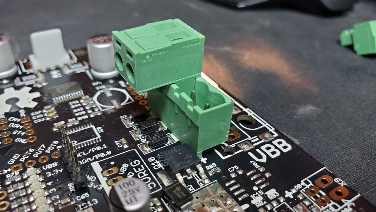
I’m leaning towards just using @analogoutput’s board myself though with a few minor changes - I moved all the traces to the backside so I can etch a single sided board for it. I eliminated the second AC terminal block. And I changed the terminals to 3.81 pitch and shifted the AC one to the edge of the board to accommodate the pluggable headers that I have and plan to use which hang off the side of the board:
My tayda parts may be here today (they were out for delivery but now show on hold) so I may be etching a board or two tonight
Oh - and I’ll be etching these on 70 x 100mm boards even though it’s only drawn as 61mm x 100mm. Which will help with the marginal size of the ground pour around D1/D2. But I may shift them to the center just so labels can be a bit more clear…though since I don’t usually bother with DIY silk and will have an extra 9mm on the top/bottom I may not bother.
There. Now all the labels are nicer. (though could still be fine tuned) No more marginal sized ground path, and every dang diode on the board faces the same direction.
Is your pluggable terminal block footprint in your version of KiCad, or did it come from elsewhere? I drew up one for mine but maybe there’s a better one out there…
I’m just using a generic terminal block footprint for now…and it’s not quite right. I need to learn how to draw up a custom footprint since I can’t seem to find one to match.
Latest version, a few position tweaks. Two pluggable AC connectors for daisy chaining, and I decided to add a barrel jack footprint so I’ll have that option, e.g. for a workbench supply.
I kind of wish I had bought vertical pluggable jacks instead of horizontal. And 5mm so I could just use yours as is
But…I think I’ll go with my revisions with the one jack in the center. Nice thing about etching my own - if I want to switch to a barrel jack I can just etch a version with that footprint instead - no need to order 5 and wait a week or two for them
And I got my bits from Tayda today with enough components to build 3 boards so looks like I will probably be doing some etching tonight.
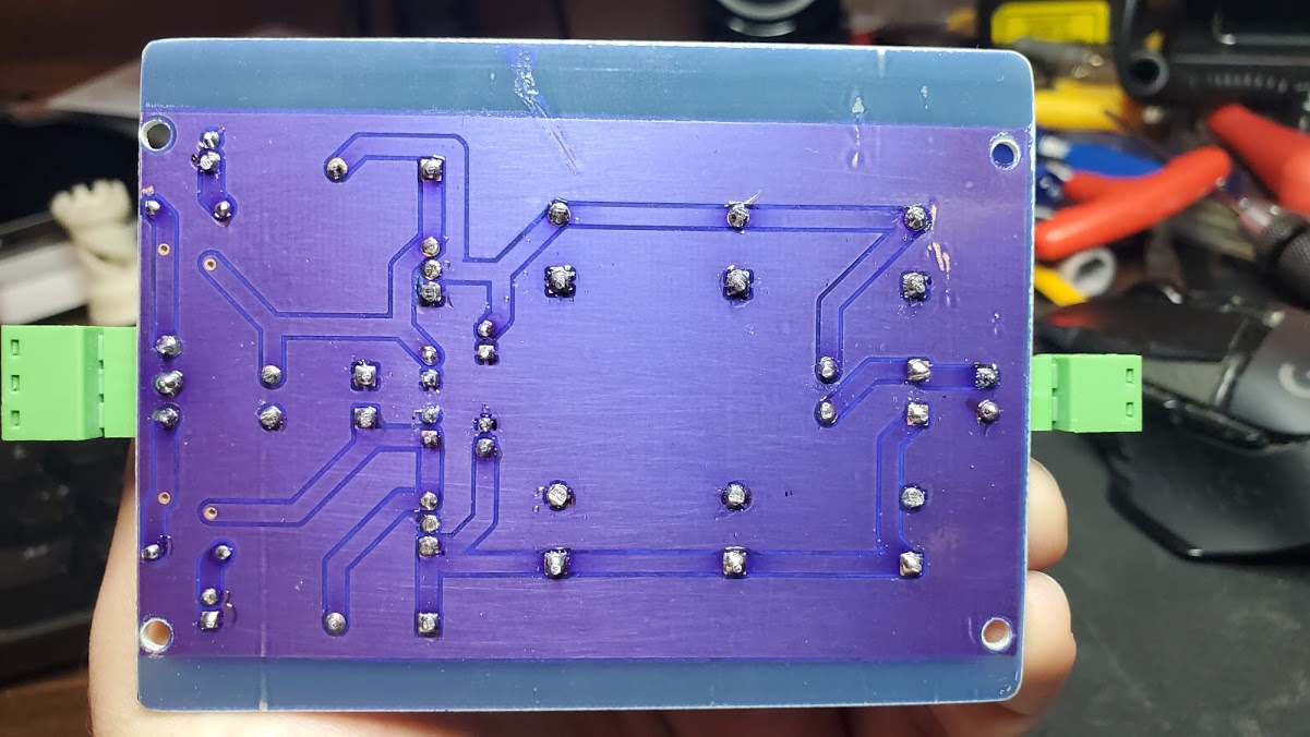
For the record…building with a backwards silkscreen is harder than not having a silkscreen at all.
Unfortunately my polyfuses that were supposed to arrive Saturday are still being held hostage by the USPS. (Actually the Amazon seller didn’t even dispatch them until Saturday and they just got into Amazon’s hands today…so should be here in a day or two.)
I could just bridge them over for now…but…I’m in no rush.
Also ordered some 5.08mm pitch terminals (and I went vertical this time) since the ones I have and used here won’t fit on my bus boards…and since I have a stack of 10 of those I’d rather get new connectors than hack that up
So from casual interest to full blown production process that can squirt out a populated board in a day while your printer whips up rails and face plates is you at what speed exactly?
Short periods of very intense activity…but leisurely spaced out
Besides…I’ve got plenty of other things to work on while I wait on this. Like wiring up that ARP4072. or printing rails for a 3rd case to replace the first one since I like these rails so much. Or wiring up the triggers for the sequencer. Or building the case/powersupply for the sequencer. And those are just synth projects off the top of my head.
I also need to spend more quality time with this Liven 8 bit warps that showed up on Friday:
This thing is pretty crazy. I’m still having a hard time figuring out how to use the looper functions. And everything the sequencer can do. But just the sound engine on it is a blast to play with, all kinds of crazy chiptune sounds in there.
Which also reminds me…I still need to debug my midibox SID and build a power supply and control surface for my midibox FM one of these days. Those have been patiently waiting close to 15 years for me to finish them
Just a matter of those bursts of activity lining up with the right projects!
Etched a new power board last night. Re-used all of the components except the regulators and the 4700uf caps (the big caps didn’t read right with either my DMM in capacitor mode or with my cheap ebay LC checker - but the smaller caps did check out and the diodes seemed fine and everything else was past the regulators so unlikely to have been affected.) Which is a bit of a bummer as those caps are the only things I don’t have spares of. Oh well, when I get to the 3rd board I’ll give them a try and see if they’re actually bad or not.
I didn’t bother with silk or soldermask this time:
Except…I’m going to do one more thing first. I’m going to make a little 3D printed plug to hold the power jack on the outside. I’m thinking something that will fit into a 1/2" hole (since that’s the biggest I can easily drill without digging out the spade or forstener bits) and hold the jack as well as 4 - 3MM LED’s so I can see the power status of both rails on both supplies from outside the case.
And build up the next power board and buss boards so the case will be fully armed and operational so I can start moving modules in. This will become my “primary case” and the old original case will be the temporary test bed until I build up another case like this one to replace it.