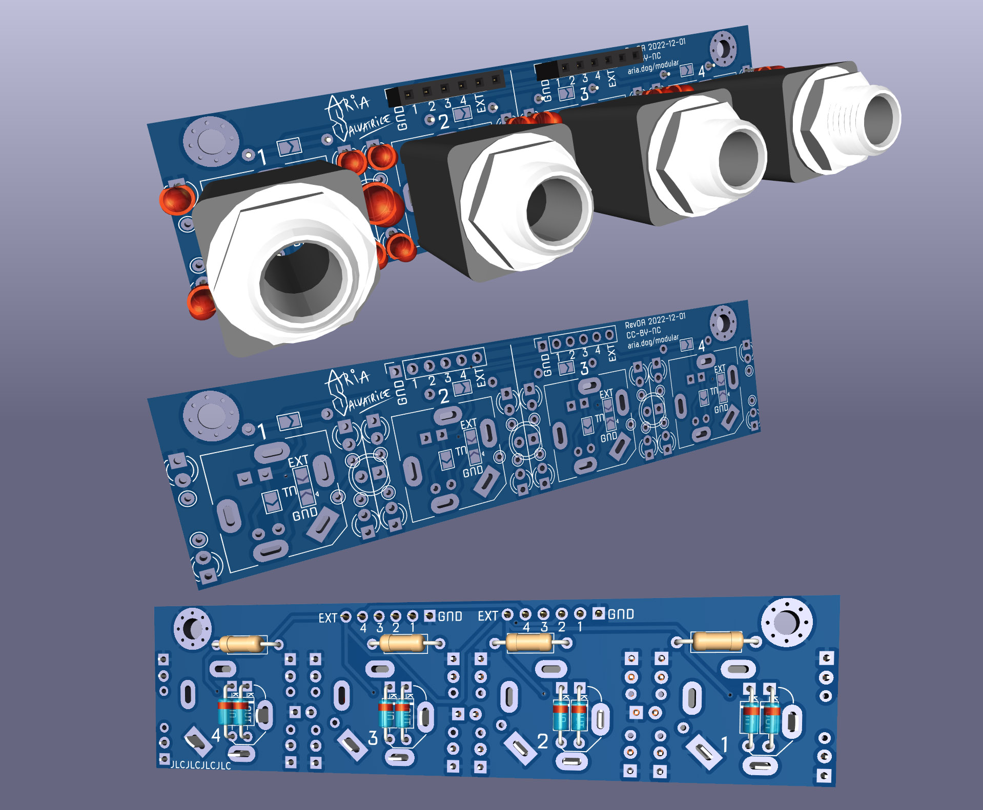
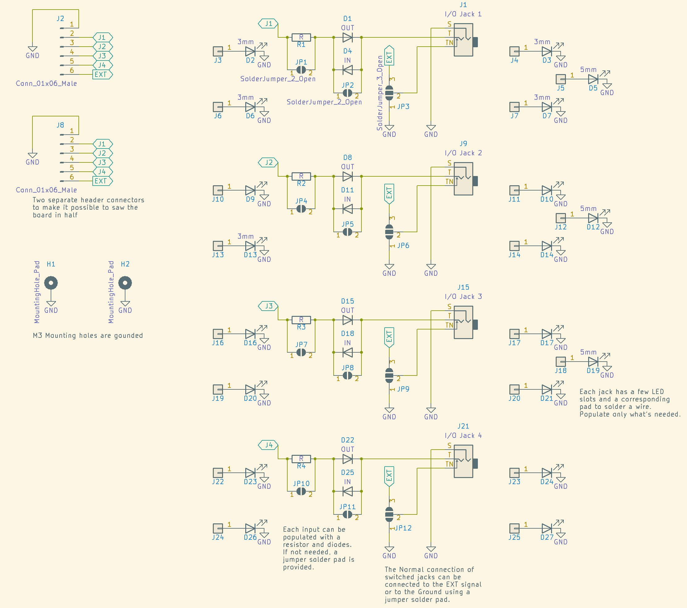
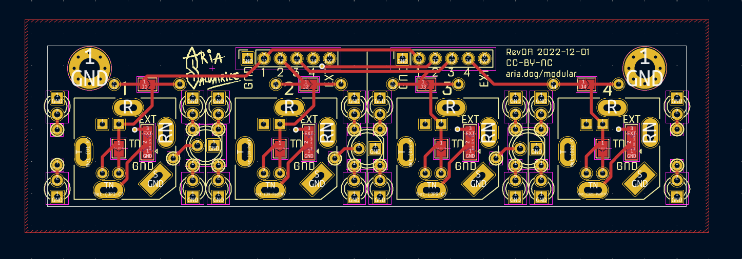
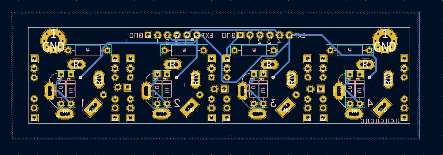
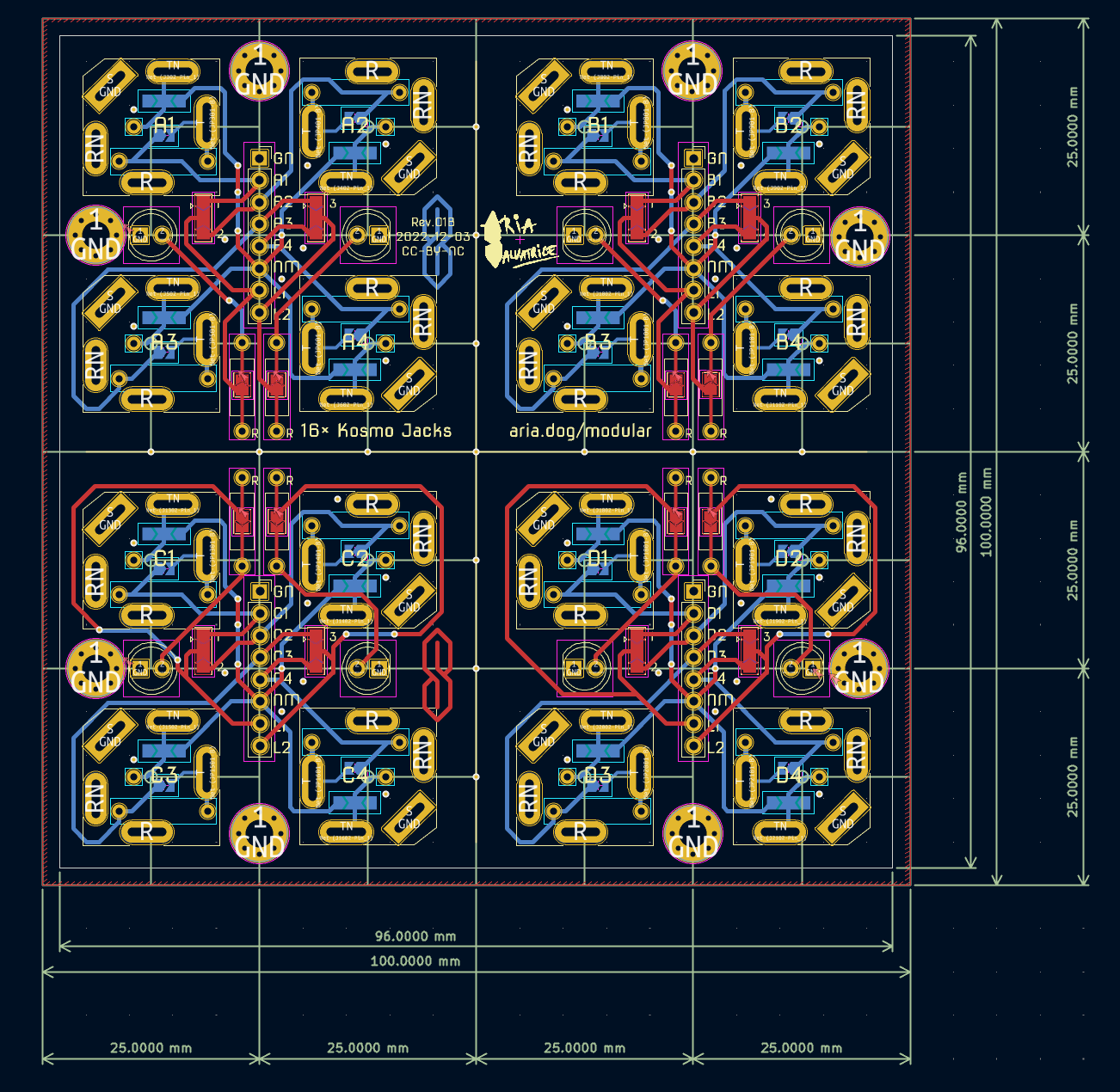
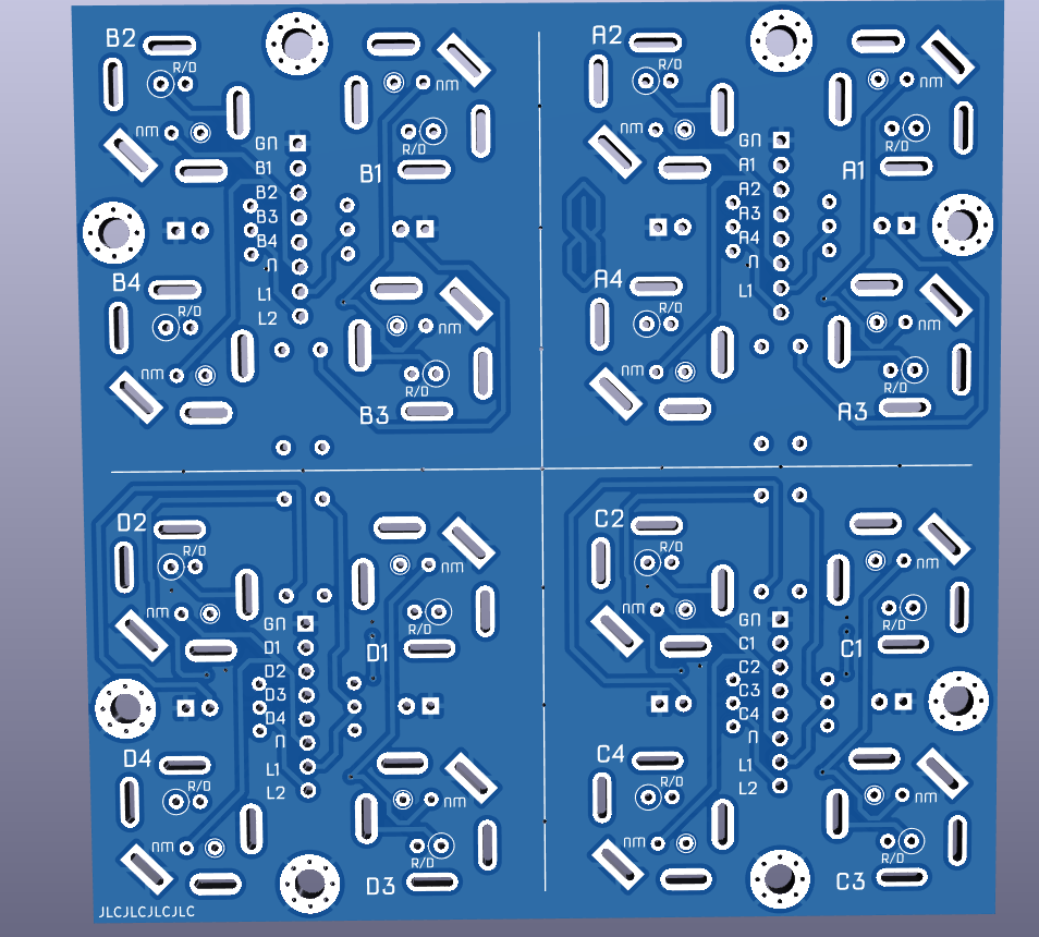
It’s very cramped but you’re only meant to populate what you need, not everything. There’s a room for a diode and a resistor per jack, since they’re commonly used there, and if skipping them, solderable jumper pads. One LED per jack is probably all I need, but multiple potential positions seem useful.
In theory it possible to split the board in half with a saw or rotary tool too. Added a pair of M3 mounting holes since there was some space left, no specific plans to use them with standoffs right now.
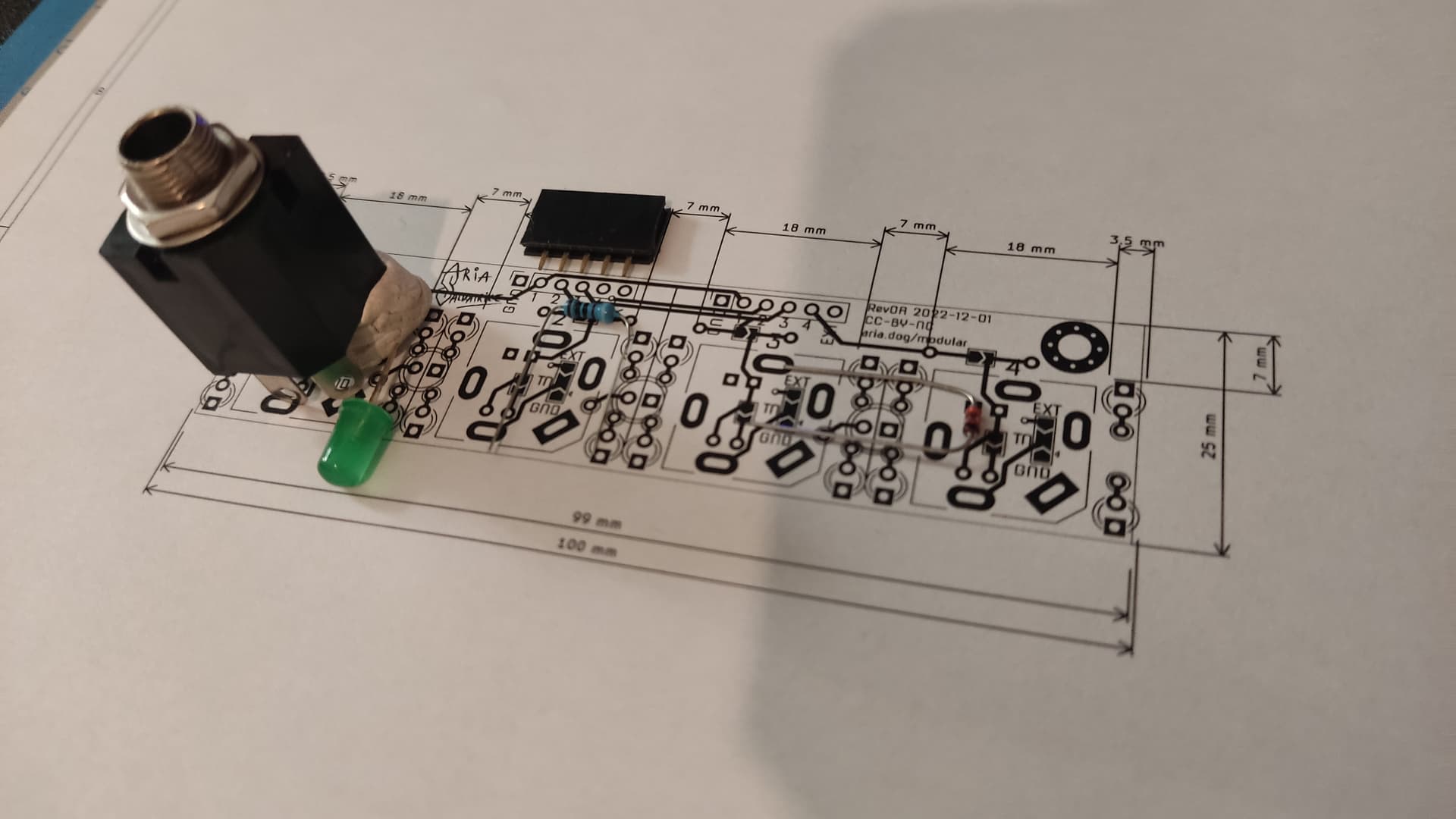
Will it work? No idea! This will be my 2nd finished original PCB so I bet I did something wrong, especially in the mechanical design aspects. So if you wanna take a quick second look, that’s welcome!
I’ll probably send it off to print tomorrow after I double-check everything.
That wasn’t a requirement, so I think it’s fine if it has to be that way, I’m not sure I can put them all in the back cleanly.
The main problem I’m seeing with LEDs as I set them up, testing with paper cutouts, is that with the height of jacks, LEDs don’t have leads long enough to have them protrude directly out of a panel. If I’ll need to use wires, no point having this many footprint options in the first place.
If I reclaim that space maybe also I could add a transistor buffer from the respective jack tips?
Depends on the LEDs; most of the ones I’ve used have leads just long enough.
Some don’t, which is what prompted me recently to go looking for (and find) a new source of diffuse bright LEDs.
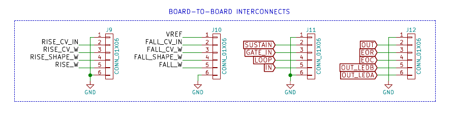
A question I’d raise is… How will you use this design? One thing is if using a single jacks board on a module you’d be limited to four jacks in a 10 cm module or two in a 5 cm module, and for most designs I think that’s too few. But you can’t use two boards having all four jacks on each on one module. Well, you could if you put one row of jacks across the bottom of the panel and one across the top. Or one up one side and one up the other. I definitely don’t like the former layout and would not want to use the latter much.
I guess you could use two jacks boards in two rows across the bottom provided the upper row has fewer than four jacks on it, and in particular one of the middle positions is empty. Then the main PCB could have a tongue extending through that position at the top jacks board to the header on the bottom jacks board. For a 5 cm module, though, you could not use a similar idea.
But I’d think an eight jacks version with two rows would be more useful. Of course if you do need only four jacks in 10 cm that would take up more room than needed, but a 10x20 cm panel usually gives you room to spare anyway.
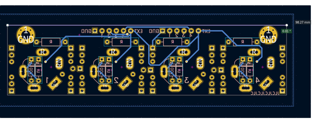
and the outer LED footprints are overhanging the edge. If so I suggest it should be made shorter. Per Kosmo Specification a width no greater than 96 mm is recommended. You don’t want to be bumping adjacent modules. I get that you wanted multiple options for LED placement but 19 footprints is I think excessive. I’d get rid of the outer ones at least.
For Kosmo I always use 5 mm LEDs so I’d reduce or eliminate the 3 mm footprints, replacing some with 5 mm. But that of course is a matter of taste.
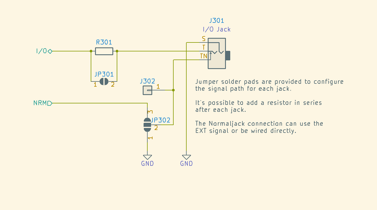
Better would be upstream end of LED series resistor to upstream end of output jack series resistor. 98% of the time that’s how you’d do indicator LEDs for outputs. For inputs you’d want some sort of buffer or driver circuit for the LED so you’d need a separate connection from the main board for that.
You could fit series resistors for both LED and output on the board above the jacks. If you use smaller resistor footprints (for 1/8 W or small 1/4 W resistors, or for standing resistors) they’ll fit even more easily.
My inclination would be to get rid of the diode footprints entirely. I use series diodes with jacks rarely enough that I wouldn’t want to have to fill in a jumper to not use one. Besides, a series diode really should have a pulldown resistor between it and the jack for output, or on the other side of the diode for input, and you don’t really have room to add those resistor footprints.
Looking through your designs on github a while ago I remember that for one of them you solved it by raising the pads using stamped contacts, too.
For one-off projects with a sufficient amount of jacks it feels justified, where the main circuit lives on a prototype board.
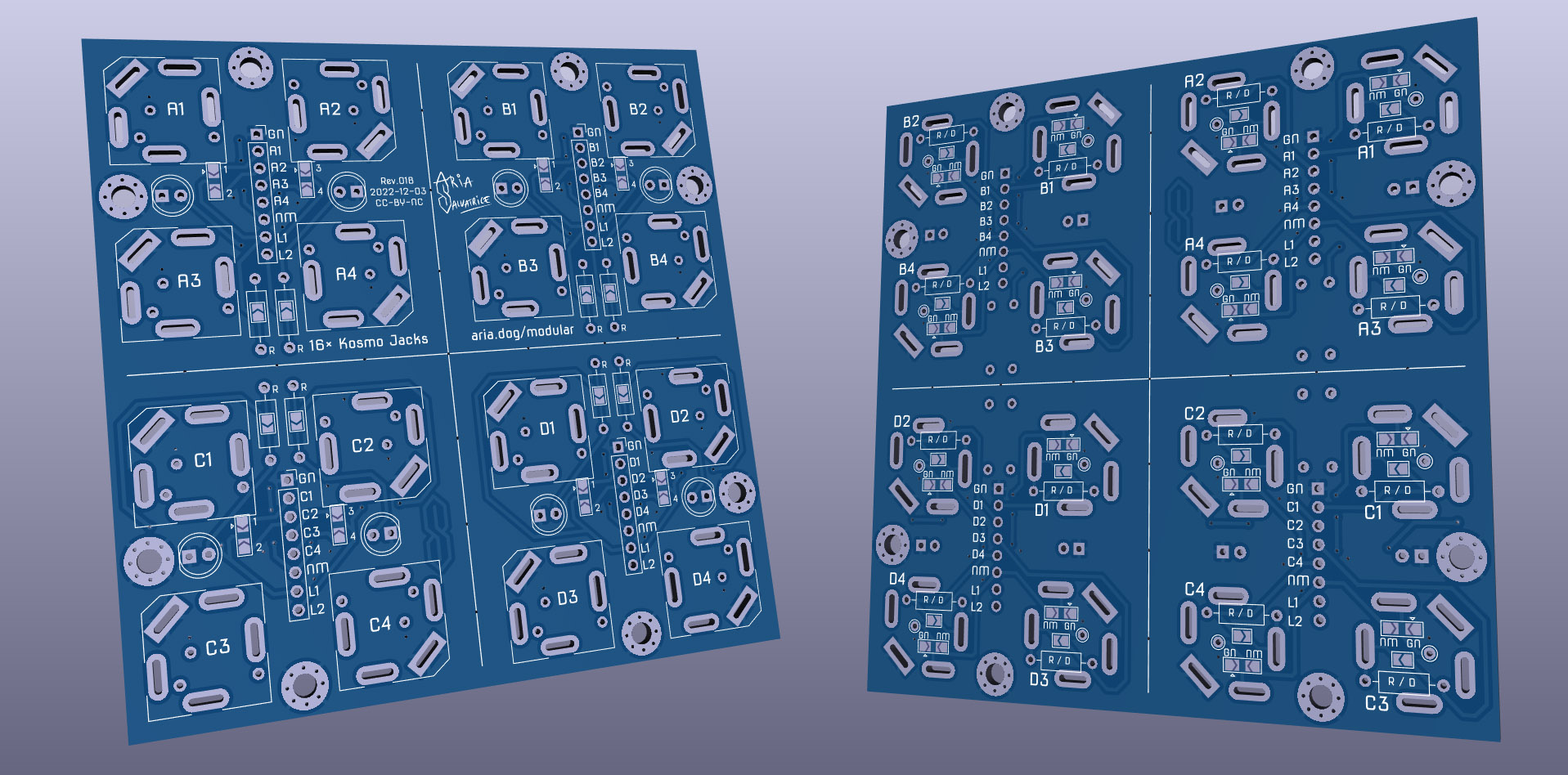
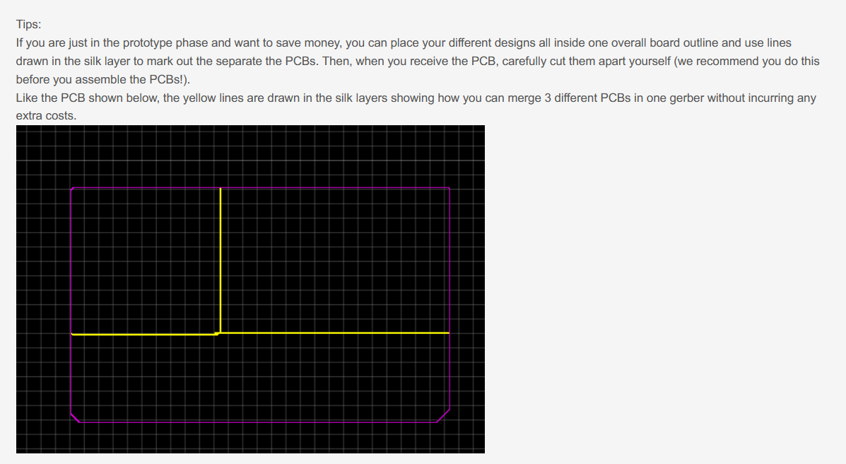
At this point, if I build expecting to cut them, maybe a 4×4 board arranged such that I can cut into 4×2×2 might be a better way to maximize the fab deals on boards below 100×100mm.
My ADSR used a 3PDT switch which is taller than a DPDT, so the panel had to sit further from the PCBs, and in that case I did need to solder a 2-position SIP socket to the LED footprint and socket the LED into that.
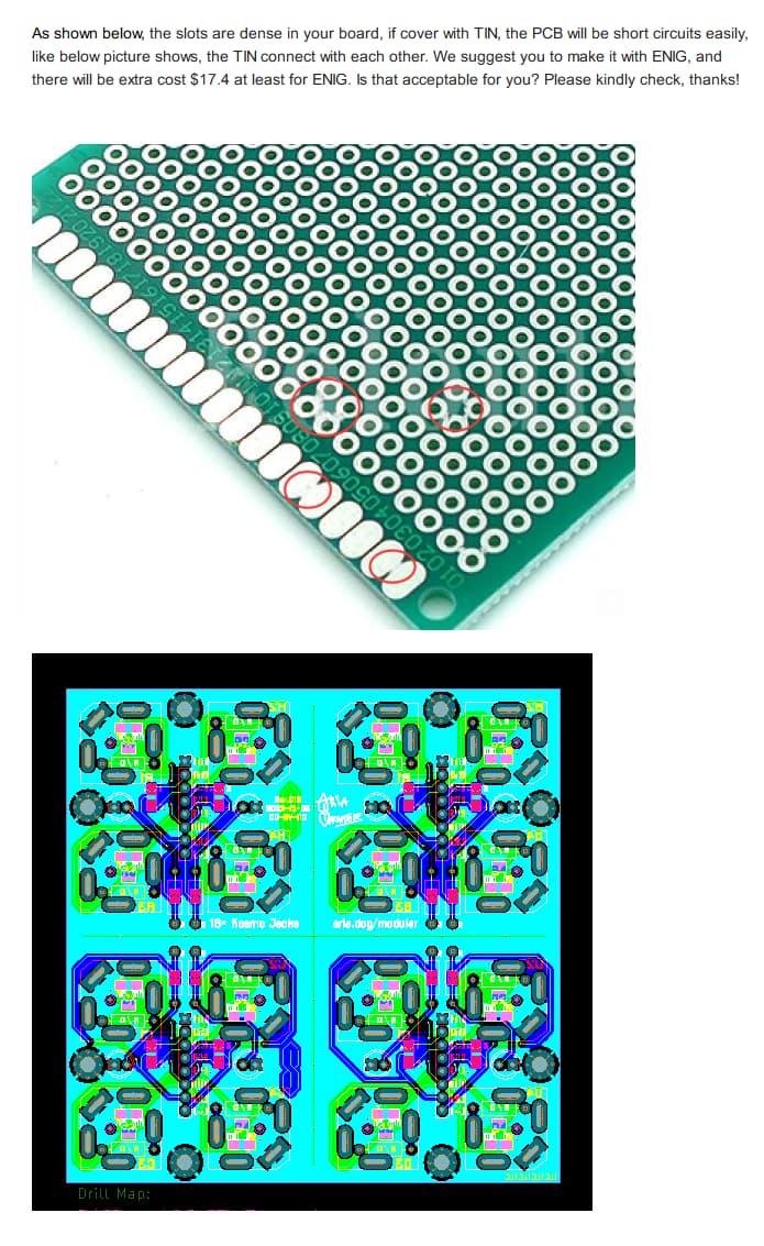
I think those solder jumpers are the problem, or maybe the slots are too close together… I sent them a revision that may or may not solve the problem ¯\_ (ツ)_/¯
I’ve done jumpers with HASL before, no problem, but they’re not that consistent with what they object to or not. They do respond to questions about the issues.
It was getting late evening in China so I just sent a revised design using normal pads close enough to bridge with solder or a cut lead, instead of waiting on an answer tomorrow heh.
I’ll look into this better and try to make a custom footprint that fits their capabilities next time.
For now I’d rather receive it fast than make it perfect, it’s meant to help me split my current project in discrete sub-assemblies & improve my PCB design skills. (They never told me how much Factorio experience translates directly to PCB routing skills lol)
Well, now they ask me for 15 currencies again, this time because there are “too many slots”. Seems they will make up a reason to add a surcharge until they find one that sticks huh?
I asked them to cancel the order for now, I’ll probably go back to this board in a few days and figure out something (like round holes - i need to cross reference with more existing projects to see what i can get away with). I want to learn design techniques that are guaranteed to make it through most fab houses without surprise surcharges.
I think it depends who handles your order, I had a panel for a 16n made up (50hp euro) with 16 slots for sliders and they added $17 onto the price. When they arrived I realised to my horror I forgot to change the solder mask color and they were green. Reluctantly ordered again a few months later and then was no additional charge.
A friend also tried to get them to fab a panel for a monome grid, which they flat-out refused to do but he kept resending the order and eventually it went through.
For future reference, as there is very little info about this on the web: If they ask for a surcharge, the UI won’t let you cancel the order, and they ignore your first message asking them to cancel, you can just tell them in the live chat you want to cancel, they did it for me immediately.
A reason it might have been refused is also that the jacks I found a good deal on are for panel mounting, so my footprints are bigger than usual. I think I’ll shelve this project until I have to place an order for proper THT jacks, but I’ll want to revisit it eventually.