Briefly, the background: About 3 years ago, having gone down the rabbit hole with Sam’s video’s during lockdown, I set off on a quest to build a “MVP” modular synth (in the Kosmo format, naturally). I found Eddy Bergman’s (excellent) site, bought a Frequency Central Microbus, a Beatstep Pro and set out to build the AS3340 VCO, the VCA (Yusynth design) and the ADSR with 7555 (as the write-up suggested that they worked well together).
I thought it would take about 3 months. Clearly that was ambitious.
Full disclosure: I’ve built a few guitar pedals but I’m definitely not an electrical engineer. This project involves (as intended) a lot of “learning-by-doing” and using freelancers on Fiverr to help me with tasks that I simply don’t have time to learn how to do myself (like PCB design).
What I’m hoping the LMNC community hive mind can help me with :
Regarding the x3 projects above, is there any reason why they wouldn’t be compatable? (Input voltages? Output voltages? etc) Eddy’s website says they are, and he seems to have a working synth (and know what he’s doing), and I’ve really no reason to believe that they’re not, but I just want to absolutely rule out this scenario.
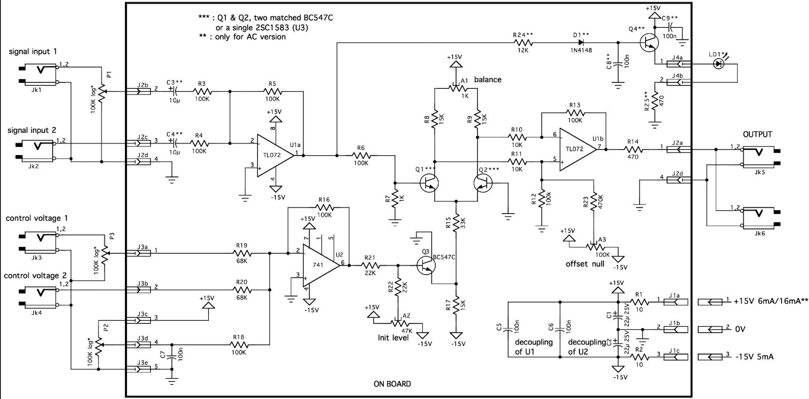
Regarding the VCA, this is my schematic and this is the schematic I was trying to copy. Is anyone able to spot any (no-doubt-obvious) errors in my translation? I’ve spent hours looking at both and can’t see any errors, but I can’t get the VCA module to function at all.
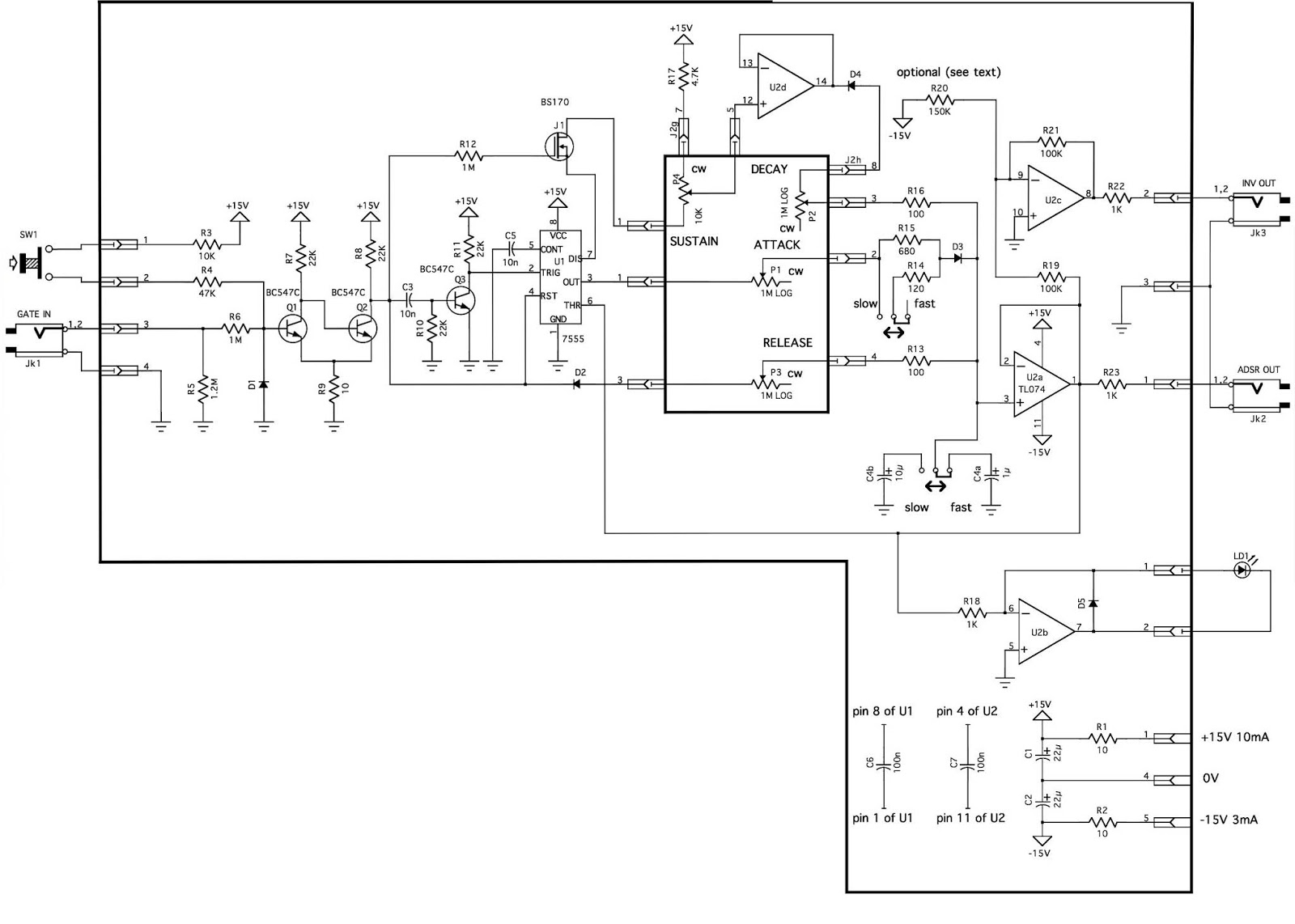
Similarly for the ADSR, this is my schematic and this is the schematic I was trying to copy. The manual trigger switch generates an envelope, but I can’t get the Gate In jack to work with either the VCA (see previous question) or any “non-DIY” Eurorack modules borrowed from friends. As before, are there any errors that anyone with (fresher, more qualified) eyes can see that I’ve missed?
I’d love to get the MVP version of the synth up and running so any help getting this over the line would be appreciated. Please ask if any further information to what I’ve included above would be helpful.
No discrepancies jump out at me. But it’s hard to know what to look for when the only symptom description is “doesn’t function at all”. More than likely something does function, the input signal probably gets to some point even if nothing makes it to the output. Using an oscilloscope or an audio probe you can try to trace down more specifically what is working and what isn’t. Have you gone through General advice for troubleshooting a module and asking for help ?
What are you expecting the VCA to do that’s relevant to the Gate In jack? The only output the VCA will produce is the amplified input signal.
One side note: Given that both schematics are pretty much just redraws of the YuSynth schematics, and that you have made them publicly available, it would be courteous to add the URLs for the originals and label the schematics as Yves Usson’s work, rather than for instance “AdamDynamic VCA-001” which makes it look like you’re trying to take credit for the design. Not your intention I’m sure, but it’s not good when schematics get passed around without attribution to the people who created them.
@EddyBergman sometimes responds here. i would imagine the modules work fine together.
Without my dual screens it’s difficult to compare the two schematics, the ADSR one I have never seen but I have a version of that VCA design in my poly6.
As Rich says you need to do some tracing of both signals and also connections.
As for paying somoen of fiver for PCB design, spend an hour designing something simple in KiCad, send it to JLC and your then on the path to enlightenment. You already seem to have the schematic so the PCB is just laying stuff out , connecting tracks ( i cheet with an autorouter) and uploading the GERBs to JLC. But obviously the Schematic needs to work before you do that!
Ok, I have 2 screens side by side here and I went over the schematics and I couldn’t find anything wrong. The ADSR schematic you made I found difficult to read at least the part with all the potmeter connections so I can’t be certain there’s no mistake there but I think it’s all fine. Did you make your own PCB designs, or you outsourced it I believe. My guess is there could be one or more mistakes in the PCB designs. Btw, what is MVP?
I’d start with an MS-20 Voltage Controlled Filter - easy build and loads of verified stripboard schematics out there → then build an AS3340 VCO, then play with that setup for a bit and think about what you want to do next, which is probably going to be the envelope generator, then the vca. Much easier to build an AD rather than ADSR and just as much fun. Along the way you’ll get your skills up, and you’ll probably want to build some more utilities, so you’ll probably want a simple op amp mixer, a passive multiple, a basic triangle LFO and a passive lowpass gate. Maybe along the way you’ll make some music!
I think an hour underestimates it, but not by that much. I went through a series of tutorial videos, a total of around 1h45m, and with the pausing to go follow along in the software I probably spent 3 or 4 hours at the end of which time I had sent a design for a (small and simple) PCB out for fabrication (and it worked). Still, in the past 3 years, I bet you could have found 3 or 4 hours to pick up a valuable skill and stop relying on paying money to strangers who may or may not be any good at it. Also, it’s fun.
Yes, a filter is an indispensable part of any (East coast style) synth and the MS-20 type design is good. It does require an LM13700 which is getting harder to obtain in through hole packaging; SMD is still in production though. I sort of infer, but am not clear, that you’re not doing stripboards but going with PCBs. You could buy the Barton PCB for $8 (BMC055 SK VCF), the pots layout is too tight for Kosmo but just move the middle one off board and you’re good. Or if you prefer you can lay out a board yourself from Barton’s schematic or René Schmitz’s, though in the latter case I’d breadboard it and work on some resistor value modifications: The input level to the LM13700 is too high for 10Vpp signals and probably the 10k input and feedback resistors should be more like 39k or above.
The BMC055 with one pot hanging off like that was the very first thing I built! I messed up my sourcing and used wildly out of spec components and it still worked fine, so it seems like a very forgiving and beginner friendly make. Plus then you’re doing an order from Barton and you can get a bunch of his other fun pcbs too.
Thanks for the many replies I’ll attempt to answer the various questions in some sort of logical order:
Indeed, as @BlackDeath mentioned it’s a Minimum Viable Product, or in this instance intended to be the smallest combination of modules that would provide a workable synth (I noticed after I made the post above that I used a similar phrase in my inaugural November 2020 forum post while still figuring out what “minimum” meant in practice).
This is an important point and worth addressing: it’s absolutely my intention to make explicit reference and give full credit to Eddy, Sam, YuSynth, etc in the “v1.0” of anything I publish online. I never intended to share the v0.x schematics or PCBs publicly and only do so here so that I can (hopefully, finally) satisfy myself that they work (ideally by getting them to work myself) and then write up the project and share with others on the same journey. I work in open source software and I’m very much a champion of proper attribution and giving others permissive licenses to re-use my own contributions to the space (however modest).
Each project has its own PCB (the gerber files for the VCA and the ADSR are in the same repo as the schematics) and faceplate, both of which I got fabbed at JLCPCB (rather than use stripboard per my guitar pedal building days, I was inspired by one of Sam’s videos where he starts to convert his synth to PCB having had one-to-many equipment failures at gigs…)
As a reference, I’ve attached photos of the PCB and faceplate for the (happily, fully working) AS3340 VCO. The green terminal blocks connect the pots to the PCB (the numbers on the schematic should correspond to the lug number on the pot). The other modules are all built in the same style.
The designer(s) who designs the PCB layout uses the same set of design files to create the schematic (i.e. both are done at once), so I assume (but worth me checking) that if the schematic is correct, then the PCB layout is correct. Please say if this is a false assumption though.
If you only have the Gerb’s it’s going to be a problem. Without the laid out schematic and associated PCB design trying to check the work done willl be laboriously goign over each pad to pad connection with a meter to verify the board is correct.
It’s false. The PCB layout can always have missing traces, or traces that intersect where they shouldn’t, or un-updated ground plane pours, or any of a number of things. KiCad has tools to help you avoid these mistakes but you have to use them.
Having said that, I think there’s a pretty strong likelihood it’s not the schematic or the PCB, but an assembly defect. Either way, the best way to find it is to trace signals and connections and see where in the circuit things go wrong. That’s a skill that takes some time and effort to develop, of course. But no time like the present to start.
I think both the VCA and ADSR PCBs were designed using Altium (the design files for the VCA are here and for the ADSR here, if either are useful).
I’ve done various spot checks of both PCBs but haven’t (yet) methodically worked through every node and vertice. Agree it would be laborious, but perhaps less laborious than building another module only to have it not work for reasons unknown.
Ah interesting, makes sense. The freelancers I used seemed to know what they were doing (some more than others) but it’s not impossible that some mistake like that slipped through the net.
I agree this is the most likely candidate. I wanted to first rule out 1. incompatability, and 2. an obvious error in the schematic (the purpose of this thread). Absent both those things, I think I need to make another one of each module, start working through the signal chain, testing voltages, etc and then report back.


