adding a 1k protection resistor in series with the buffer outputs (and connecting the outputs to the tip, @twinturbo you’ve got one connected to the sleeve)
adding a negative offset to the outputs so that they swing positive and negative (the outputs of the 3340 only go above ground)
adjusting the output buffer gains so that the output signals have the same amplitude
It’s also interesting that neither of you is using the pulse output from the 3340.
Do you intend to generate a pulse output from the triangle wave with a comparator? That’s what I would do.
I disagree, the schematic is much easier to read and less prone to error with the proper component symbols.
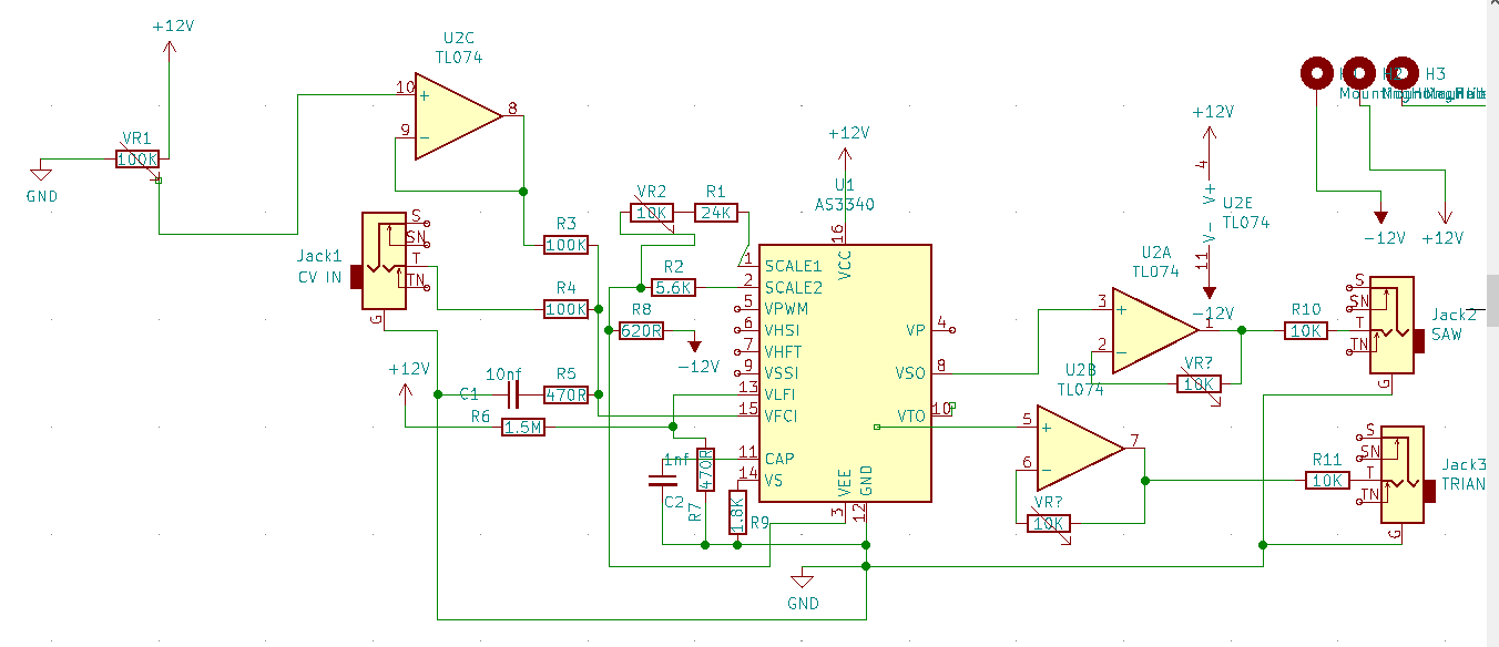
Ok, So hopefully I have understood the sugestions from Fredrick & Antonie…
I should point out that the omission of anythign fancy is down to both diagrams being direct replicas of the sketch on the website projects page.
I have swapped out the TLO72 for a 74 in order to accommodate the revised input stage.
Added 10k’s on the output stage
Corrected the 100K trimmer to be 10K
Corrected the jack that was on the sleve and not the tip.
Added some pots on the feedback on the output OP-Amps ( hope this is correct )
Onlything I was not sure on was the “Adding Negative Offset…”
Yeah, I was a bit reluctant to suggest things that weren’t part of the stripboard, because then it’ll never end (and you should just order the performance VCO instead, and modify that before building, and…).
But just a note that U2C isn’t strictly needed (none of the LMNC designs have it), even if it adds a bit more isolation between pot and summing resistor, making things more linear. But if you keep it in, make sure not to leave the input to the fourth opamp floating; connect +in to ground and −in to the output (i.e. wire it as a voltage follower with 0 V in). If left unattended, it may do silly things and interfere with the other opamps.
(and those VR things still look weird to me, at least VR1 and VR2 ).
Well yes…it is deviating a little… I already have the performance VCO (not quite finished) I just wanted to get my head arround the design aspects and it was a simpler example than the one on the data sheet.
In regards to U2C it was included as it’s show on the 1V/o input on the performance VCO… But if it’s not needed I may delete it. But thank for the advice on the 4th OP-AMP, it’s little things like that which may never be obvious…
I think it’s almost ready then to do the final PCB and push out to JLC… I sent them 3 designs for other stuff yesterday so this VCO can go on another order with a couple of other things…
That’s quite high, the 1k that I had suggested should be enough to protect the outputs against short circuits.
Good.
If that was in regards of my comment, it won’t cut it.
You can check out this one minute primer on opamps if you want to get started with opamp circuits and figure out why just adding pots in the buffers’ feedback loops won’t do anything. Hint: you can’t have a voltage divider with only one resistor.
Beware also, that pot symbol is tricky, if you made a PCB from this schematic, the wiper of the VR? pots would not be connected, so your pots would just be fixed resistors.
Think of it this way: you can replace the output buffer by a simple mixer and “mix” in a fixed voltage: the offset you want to add (or subtract).
VR1 looks like it’s supposed to be a potentiometer, with three wires connecting to it, and not a variable resistor, in which case it is the wrong symbol.
VR2 seems okay but there’s a weird wiring path below it that could use some straightening out.
That’d depend on what footprint you use, and in fact I can’t find a variable resistor footprint in the standard KiCad libraries even though there is a variable resistor symbol in the symbol libraries.
In fact maybe such a footprint isn’t possible, since it’d involve adding a wire trace to a potentiometer, and I don’t think KiCad footprints can include wire traces, or can they?
@analogoutput
Ahh indeed the symbol is just a variable resistor, this was the first schematic I sketched out in KiCad, and must have gone with variable resistor for the symbol. It looked like it was connected but the PCB rats nest says otherwise… That’s corrected.
@antoine.pasde2
I need to go back and read that “One minute op amp analysis” a minute must be longer in the USA I found the section in Ray Wilsons book also so will have to have a proper read of that.
I note that the output on the Performance/Tuner VCO has neither the Bias or Amplitude, something tells me the question of the amplitude has been
@Everyone
Thanks for the input. I am getting to grips with all the functions in KiCad, Fusion360 and Inkscape and it’s a great distraction from daily life (Actually I should be working right now but my heads not there ).
It’s actually a Canadian site.
You’d think the cold would slow them down, but apparently not.
Actually the guy’s from Toronto, it doesn’t really get cold there. (I know, I’m from Montréal.)
LOL… I remember back in the 90’s I bought a 3.5" Floppy Drive from “Evesham Micros” it did not work and I spoke to a guy and he gave advice… I rang back later and said it still did not work
Me… “I spoke to an American guy, he said XYZ…”
Guy “That was me,… I am Canadian actually”
anyhoo… drive still did not work despite continental warfare…
as for the output… I can’t rememberm it’s been a frantic few weeks… But looking at the LFO it’s just a straight output from the 3340 via a 072… I seem to recall looking or seeing a post regarding this as the 3 waveforms have differing output characteistics… I would think i am imaginig it, but that would meand i have understood the data sheet too well!!!
I’m glad I searched this time instead of blind posting… I just got finished drawing up a similar schematic in kicad before I thought to search first. but I can’t find anything still. but I’m so new and inexperienced that the rats nest is overwhelming…
Plus I know I’m not that great at it.
But I tried to convert the full board (minus the FM and Sync)… here’s what I managed
Please be gentle, I’m aware it’s messy, honestly the rats nest is more intimidating. I am working on the rats nest/routing first, if I can at least print a good set of traces for etching, then I’ll take the time to clean it all up. Honestly I just wanted to get it working so I could just print this circuit.
Instead of global labels for ground and ±12V I would recommend using the power symbols (click on the ground symbol icon on the right). They won’t change the connectivity of any PCB you make from this but they’re needed for the rules checker to do a good job, and that’s a good thing.
It’s common practice to put a 1k resistor in series between the output op amps and the output jacks. It limits current in the event the output jack is shorted to ground or a rail.
It’s very confusing having U2B on the right like that. Generally it’s good to have inputs on the left and outputs on the right.
It’s also good for references and values to be legible, so rearranging the stuff around pins 11–15 to keep them from overlapping symbols would be good. Likewise having “R13” in the middle of R12 is a recipe for confusion.
Of course the op amps need to be connected to ±12V.
The pots don’t have values shown. Or rather their values have been set to things like “Coarse_Tune”. It’s already clear what the pots are for from the global labels on them, but if that’s not enough for you, use the text tool to add a description and use the component value field for what it’s meant for, to tell if these are B100k or what. Likewise I don’t like using the value field for labels on the jacks, mainly because it’ll mess up a BOM when you generate one.
There’s some inconsistency in how you write your values, e.g. R5 is 470r while R10 is 620R. That kind of thing can mess up a KiCad-generated BOM, so it’s best to be consistent. Capital R is what I see much more often than lowercase. SI prefix abbreviations k, n, and M should be lower, lower, and uppercase respectively, so good job there! But f for farad should be uppercase (so nF for nanofarad) if you want to be completely correct (which many people aren’t, and really it only matters to nitpickers like me — except that m for milli and M for mega should not be mixed up — I suppose p for pico and P for peta shouldn’t, either, but not much chance of someone using a petafarad cap by mistake).
The rules checker when you use it will complain about pin 3 on RV1 unless you either mark it as unconnected, or connect it to 2 as is commonly done for variable resistors, but better yet is to connect it to ground and make it into a voltage divider — it’s not shown that way on Sam’s stripboard but it’s the better way to do it. Unused pins on the 3340 also should be marked as unconnected. (The x icon on the right.)
Oh wow, I really appreciate the time you took to type that up. I really wasn’t expecting anything, so thank you for that!
This is only the second PCB I’ve ever done in kicad, the first one was done along side someone showing me how to use the program since I’ve never done PCB design before. I’m in the process of cleaning it up now and will keep everything in mind while fixing the current mess
Here is the cleaned up version, or at least, a better version. I hope this addressed the issues you brought up, as well as made it easier to read.
EDIT: Granted, I just thought about, I should’ve stacked the outputs… didn’t think of that until now.
Looking good! A few power labels yet to be changed over.
Now, if this is going to become a PCB and not just an exercise, it’ll need a power header and associated components (including bypass caps by the op amp chips); they’re left off Sam’s stripboard layouts for whatever reason. There’s a whole topic about that: Typical module power circuit. For Kosmo or Eurorack formats, but if you’re doing something else it’s only the header itself that might be different.
And offsets so the outputs are centered on zero would be good too. But then we’re entering the realm of improving the circuit and there’s a good deal more of that possible: 1222 Tuner VCO Module fixes/improvements focuses on the 1222 module but most of it is applicable to stripboard versions too.
Ah yes, I see the labels now… whooops, I thought I’d grabbed them all(late nights are killer on focus XD)
I just got up and getting caffeinated, so I’ll be working on this, trying to fix the points you guys have brought up!
As to adding gain to the triangle and saw as @sebastian mentioned, I haven’t tried that on the previous build, might be worth it to set the gain rather than buffer.
I appreciate the compliments Analog! It means a lot! Especially since I know I’m so new, and I myself, have plenty of room for improvements
As to the power header, that is something I just plain forgot to put in, so that’ll be on the update. To save messages and to prevent spam though, I’m saving this message as a draft and will finish it when I’ve improved something lol.
Okay, I’ve made some improvements (hopefully), I added the decoupling / filtering caps to power, fixed the ground labels that I missed before, added gain to both triangle and ramp out.
The only thing that is bugging me a lot, is that none of the connectors, had the numbers starting from bottom, but I guess that doesn’t matter as long as the pin-out is correct.

 ).
). I just got finished drawing up a similar schematic in kicad before I thought to search first. but I can’t find anything still. but I’m so new and inexperienced that the rats nest is overwhelming…


